We can detect roughness at a 20 x 20 µm scan in Z height mode down to Angstroem level. We use nonotips silicon based. If you want to analyse your surface quality, impurities on your surface and or defects, we are able to see from 20 µm large objects down to 0,1 nm. The size of the sample can be up to 100 x 100 mm and about 20 mm thick or as small as 1 x 1 mm.
If you need just one analysis or series of some 100, please contact us for a quotation. You can receive your scan data in print or CD format or by email.
Atomic Force Microscope
Tip of AFM
Analytical - AFM
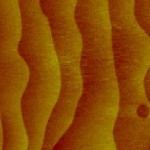
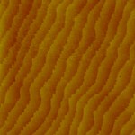
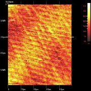
AFM of stepped surface of an Al2O3 wafer after O2 annealing
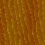
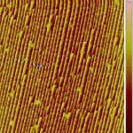
AFM of different SrTiO3 substrates after Ti - termination
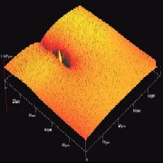
AFM of an Al2O3 wafer with GaN layer and a deep defect
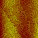
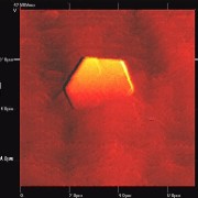
AFM of a GaN single crystal grown out of a GaN layer
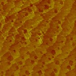
AFM of a GaN crystal grown through a GaN layer
AFM ofa GaN layer with growth defects resulting out of scratches in the Al2O3 substrate
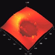
AFM of a GaN layer with a large defect resulting out of resin remains on the substrate
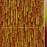
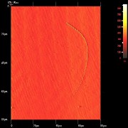
AFM of a scratch made by handcleaning on a Al2O3 substrate
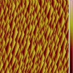
AFM of BaTiO3 substrate with lamellas out of phase transition Stress